Can I Use a 3 Way Switch as a Single Pole
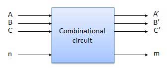
Combinational Circuits
Combinational circuit is a circuit in which we combine the dissimilar gates in the circuit, for example encoder, decoder, multiplexer and demultiplexer. Some of the characteristics of combinational circuits are following −
-
The output of combinational excursion at any instant of time, depends only on the levels present at input terminals.
-
The combinational circuit do not use any memory. The previous state of input does not have any result on the present state of the circuit.
-
A combinational circuit can have an n number of inputs and yard number of outputs.
Block diagram
Nosotros're going to elaborate few of import combinational circuits as follows.
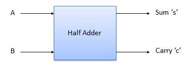
Half Adder
One-half adder is a combinational logic circuit with two inputs and two outputs. The half adder excursion is designed to add ii single chip binary number A and B. It is the basic edifice block for addition of two unmarried bit numbers. This circuit has two outputs conduct and sum.
Block diagram
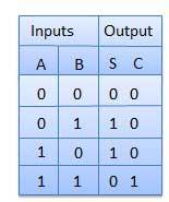
Truth Table
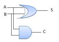
Circuit Diagram
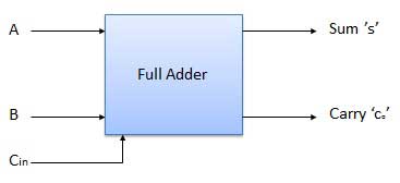
Full Adder
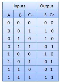
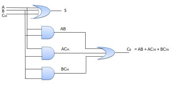
Total adder is developed to overcome the drawback of One-half Adder circuit. It can add together 2 1-scrap numbers A and B, and carry c. The full adder is a three input and two output combinational excursion.
Block diagram
Truth Table
Circuit Diagram
North-Bit Parallel Adder
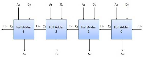
The Full Adder is capable of adding only ii single digit binary number along with a carry input. But in applied we need to add binary numbers which are much longer than just ane bit. To add 2 n-flake binary numbers we demand to use the northward-flake parallel adder. It uses a number of full adders in cascade. The deport output of the previous full adder is continued to comport input of the next full adder.
4 Bit Parallel Adder
In the block diagram, A0 and B0 represent the LSB of the 4 bit words A and B. Hence Full Adder-0 is the lowest stage. Hence its Cin has been permanently made 0. The residuum of the connections are exactly same as those of n-scrap parallel adder is shown in fig. The four fleck parallel adder is a very mutual logic excursion.
Block diagram
N-Chip Parallel Subtractor
The subtraction can be carried out by taking the one's or 2's complement of the number to exist subtracted. For example we tin can perform the subtraction (A-B) by adding either 1's or 2's complement of B to A. That means we can use a binary adder to perform the binary subtraction.
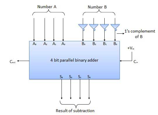
4 Bit Parallel Subtractor
The number to be subtracted (B) is offset passed through inverters to obtain its 1'south complement. The four-scrap adder then adds A and 2's complement of B to produce the subtraction. Siii Sii S1 S0 represents the consequence of binary subtraction (A-B) and behave output Cout represents the polarity of the result. If A > B then Cout = 0 and the consequence of binary course (A-B) then Cout = one and the result is in the 2's complement grade.
Block diagram
Half Subtractors
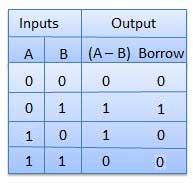
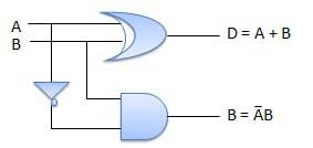
Half subtractor is a combination excursion with two inputs and 2 outputs (departure and infringe). It produces the difference between the two binary $.25 at the input and too produces an output (Borrow) to signal if a one has been borrowed. In the subtraction (A-B), A is chosen as Minuend fleck and B is called every bit Subtrahend bit.
Truth Table
Circuit Diagram
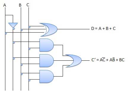
Full Subtractors
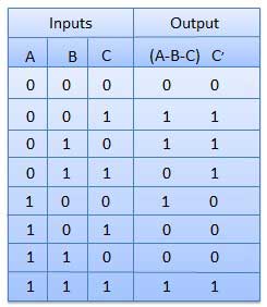
The disadvantage of a one-half subtractor is overcome past full subtractor. The total subtractor is a combinational circuit with three inputs A,B,C and 2 output D and C'. A is the 'minuend', B is 'subtrahend', C is the 'borrow' produced by the previous phase, D is the divergence output and C' is the borrow output.
Truth Table
Circuit Diagram
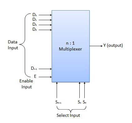
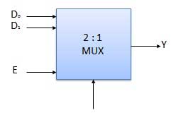
Multiplexers
Multiplexer is a special type of combinational circuit. There are n-information inputs, 1 output and m select inputs with 2m = n. It is a digital circuit which selects one of the north data inputs and routes it to the output. The choice of i of the n inputs is done by the selected inputs. Depending on the digital code applied at the selected inputs, 1 out of north data sources is selected and transmitted to the single output Y. Due east is chosen the strobe or enable input which is useful for the cascading. Information technology is generally an active low concluding that means it volition perform the required performance when information technology is low.
Block diagram
Multiplexers come in multiple variations
- 2 : ane multiplexer
- 4 : 1 multiplexer
- sixteen : 1 multiplexer
- 32 : 1 multiplexer
Block Diagram
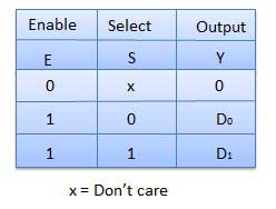
Truth Table
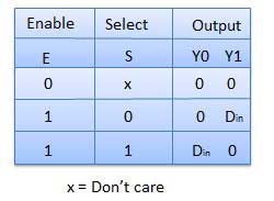
Demultiplexers
A demultiplexer performs the reverse operation of a multiplexer i.e. it receives 1 input and distributes it over several outputs. Information technology has just 1 input, n outputs, thousand select input. At a fourth dimension only one output line is selected by the select lines and the input is transmitted to the selected output line. A de-multiplexer is equivalent to a unmarried pole multiple manner switch as shown in fig.
Demultiplexers comes in multiple variations.
- i : 2 demultiplexer
- 1 : iv demultiplexer
- 1 : 16 demultiplexer
- 1 : 32 demultiplexer
Block diagram
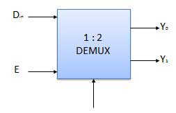
Truth Table
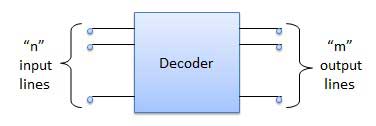
Decoder
A decoder is a combinational circuit. It has due north input and to a maximum m = 2n outputs. Decoder is identical to a demultiplexer without any information input. It performs operations which are exactly opposite to those of an encoder.
Block diagram
Examples of Decoders are following.
- Code converters
- BCD to 7 segment decoders
- Nixie tube decoders
- Relay actuator
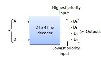
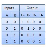
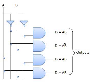
2 to 4 Line Decoder
The block diagram of 2 to 4 line decoder is shown in the fig. A and B are the two inputs where D through D are the four outputs. Truth table explains the operations of a decoder. It shows that each output is 1 for only a specific combination of inputs.
Block diagram
Truth Tabular array
Logic Circuit
Encoder
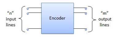
Encoder is a combinational excursion which is designed to perform the inverse operation of the decoder. An encoder has due north number of input lines and chiliad number of output lines. An encoder produces an m fleck binary code corresponding to the digital input number. The encoder accepts an n input digital word and converts it into an yard bit another digital word.
Block diagram
Examples of Encoders are following.
- Priority encoders
- Decimal to BCD encoder
- Octal to binary encoder
- Hexadecimal to binary encoder
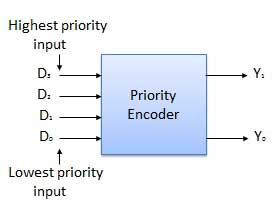
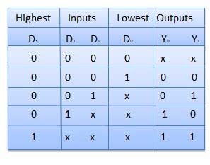
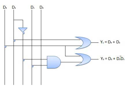
Priority Encoder
This is a special type of encoder. Priority is given to the input lines. If two or more than input line are one at the same time, then the input line with highest priority will be considered. There are four input D0, D1, D2, D3 and ii output Y0, Yi. Out of the iv input D3 has the highest priority and D0 has the lowest priority. That ways if D3 = ane then Y1 Yane = 11 irrespective of the other inputs. Similarly if D3 = 0 and Dtwo = i and then Y1 Y0 = x irrespective of the other inputs.
Block diagram
Truth Tabular array
Logic Circuit
Useful Video Courses

Video

Video

Video

Video

Video

Video
Source: https://www.tutorialspoint.com/computer_logical_organization/combinational_circuits.htm
0 Response to "Can I Use a 3 Way Switch as a Single Pole"
Post a Comment